


- 2024-05-09 14:40 1019
- 产品价格:面议
- 发货地址:广东深圳 包装说明:不限
- 产品数量:9999.00 个产品规格:不限
- 信息编号:182168478公司编号:15442499
- 郑主管 微信 13265447518
- 进入店铺 在线留言 QQ咨询 在线询价
龙鼎微耳放芯片 高品质耳放芯片龙鼎微PAM8908耳放芯片HT4832
- 相关产品:
PAM8908:25MW功率:25mw较小包装:3000品牌:pam库存情况:现货
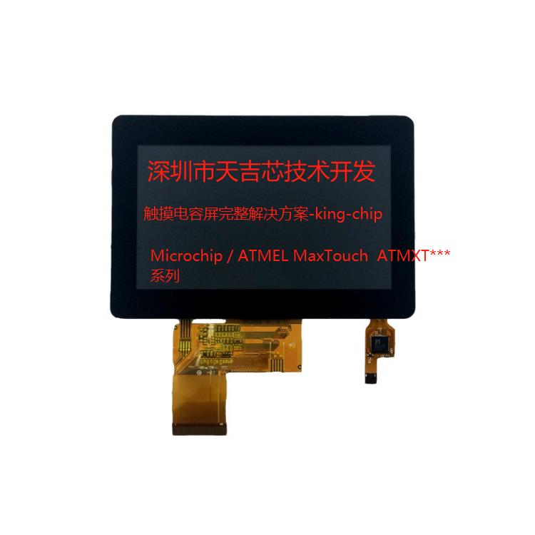
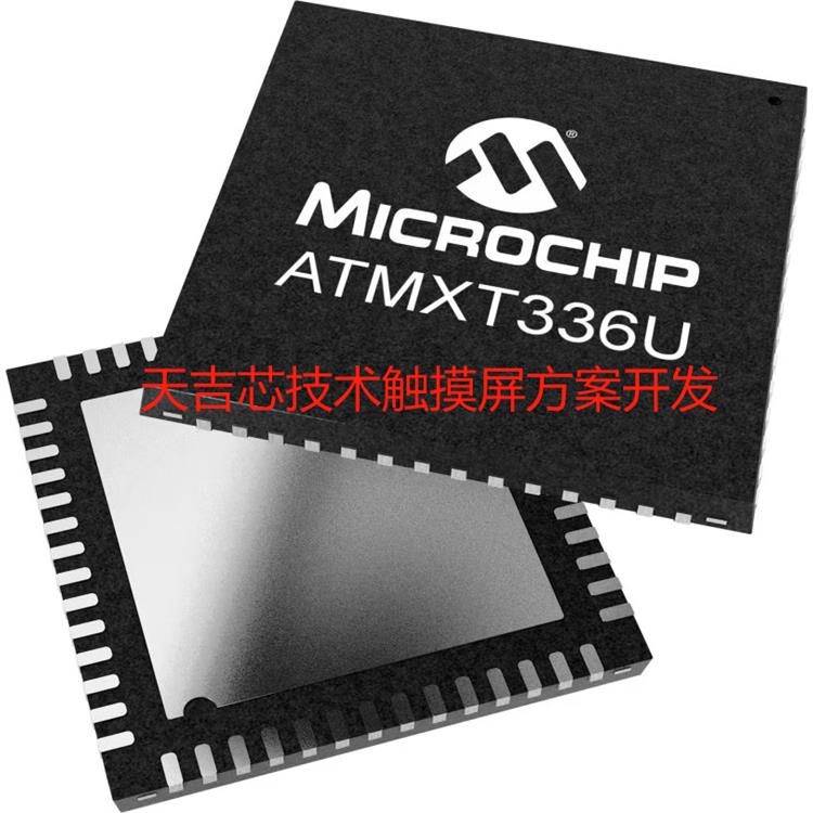
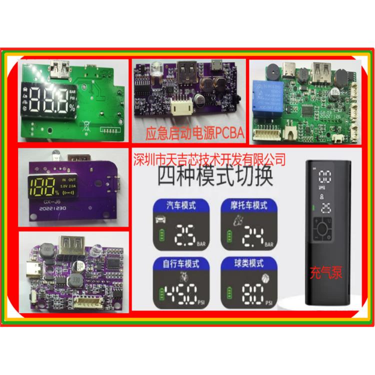
深圳市天吉芯技术开发有限公司()是一家从事消费类产品设计、集成电路推广销售,及方案开发的高科技企业,代理、分销**电子元件厂家的各类产品(MCU,音频IC--功放IC,耳放IC,DAC-ADC-CODEC,视频处理IC,电源IC,运放IC,MOS等功能的集成IC 如/index.php?m=selection&a=index&classify_id=271), 与各大原厂和代理商都保持着密切的合作关系(TI,ADI,NXP,ST, 中国台湾立錡,新唐,禾润,智浦欣,茂田MOS)。致力于打造一个能为电子成品生产厂家提供的供应平台,积累多年的水平、扎实基础及业界信誉得以快速和健康的发展。功放芯片,耳放芯片,运放芯片,电源芯片,MCU单片机等所涉及的产品广泛应用于蓝牙音响、拉杆音箱、迷你音箱、桌面多媒体音响、Soundbar 音响、耳机放大、便携式收音机、 PDA 、电视机、 儿童故事机、玩具、礼品等产业 。
AB类音频功放芯片
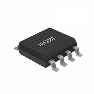
MIX2002 ,MIX2071
D类内置升压功放芯片
MIX2908 ,MIX3902 ,MIX3903
D类音频功放
MIX2037,MIX2052,MIX2606,MIX3001,MIX3006,
MIX3007,MIX3015,MIX3015A,MIX3022,MIX3605,MIX3806
F类内置升压功放芯片
MIX2901,MIX2902,MIX2909,MIX2910,
MIX2915,MIX3901,MIX3906
F类音频功放芯片
MIX2008,MIX2015A,MIX2018A,MIX2029,MIX2051
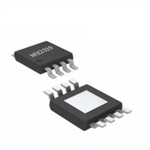
MIX2807,MIX2808,MIX3018,MIX3805,MIX2039
电源管理芯片
MIX6001,MIX6003,MIX6201 ,LP28400AQVF 微源充电IC
耳放芯片
PAM8908,HT4832,TPA6132
AT8031 2.1声道功放IC
TP358 SOP8 3PEAK运放IC
AT45DB041D-SU ATMEL FLASH
ATTINY88-AU ATMEL MCU
我司承接智能方案定制开发MCU的智能产品/index.php?m=product&a=details&content_id=62),5.8G/2.4G无线音频传输方案,无线灯控方案,从进口品牌ST的32位和8位MCU的方案开发,详情请联系:* ( VX同号),到国产的32位和8位MCU的产品软硬件开发,高品质的无线音频传输方案客制化开发,2.4G,蓝牙,Wifi,433,AI语音识别等无线智能控制单元产品。涉猎产品领域:家庭影院,无线乐器传输, 智能家居控制单元,智能灯控等诸多成熟的项目。
Diodes Incorporated and its subsidiaries reserve the right to make modifications, enhancements, improvements, corrections or other changes
without further notice to this document and any product described herein. Diodes Incorporated does not assume any liability arising out of the
application or use of this document or any product described herein; neither does Diodes Incorporated convey any license under its patent or
trademark rights, nor the rights of others. Any Customer or user of this document or products described herein in such applications shall assume
all risks of such use and will agree to hold Diodes Incorporated and all the companies whose products are represented on Diodes Incorporated
website, harmless against all damages.
Pin Descriptions
Pin Number
Pin Name I/O/P Function
PAM8901 PAM8908
1 1 INL- I Inverting left input for differential **s. 2 2 INL+ I Non-inverting left input for differential **s.
3 3 INR+ I Inverting right input for differential **s. 4 4 INR- I Non-inverting right input for differential **s. 5 6 G0 I Gain select bit 0 6 7 G1 I Gain select bit 1
7 5 OUTR O Right headphone amplifier output. Connect to right terminal of headphone jack.
8 8 HPVSS P
Charge pump output and negative power supply for output amplifiers; connect 1µF
capacitor to GND
9 10 PGND P Power Ground
10 9 CAP- O Charge pump negative flying cap.
11 11 CAP+ O Charge pump positive flying cap.
12 14 PVDD P Power VDD.
13 12 HPVDD O Positive power supply for headphone amplifiers. Charge pump positive half VDD output.
14 16 OUTL O Left headphone amplifier output. Connect to left terminal of headphone jack.
15 15 SGND I Amplifier reference voltage.
16 13 EN I Amplifier enabled. Connect to logic low to shutdown; connect to logic high to activate

The input impedance, RIN, is dependent on device gain. Larger input capacitors decrease the corner frequency. See the following table for input
impedance values.
G0 Voltage G1 Voltage RIN
≤0.6V ≤0.6V 26.4kΩ
≥1.4V ≤0.6V 19.8kΩ
≤0.6V ≥1.4V 16.5kΩ
≥1.4V ≥1.4V 13.2kΩ
For a given high-pass cutoff frequency, the minimum input coupling capacitor is found as:
Power Supply Sequencing
Use input coupling capacitors to ensure inaudible turn-on pop. Activate the PAM8901 / PAM8908 after all audio sources have been activated and
their output voltages have settled. On powerdown, deactivate the PAM8901 / PAM8908 before deactivating the audio input source. The EN pin
controls device shutdown: Set to 0.6V or lower to deactivate the PAM8901 / PAM8908; set to 1.4V or higher to activate.
TrueCapFree Headphone Amplifiers
The TrueCapFree amplifier architecture operates from a single supply voltage and uses two internal charge pumps to generate a positive supply
and a rail for the headphone amplifier. The output voltages are centered around 0V and are capable of positive and negative voltage swings as
shown in the following drawing.
TrueCapFree amplifiers require no output DC-blocking capacitors. The headphone connector shield pin connects to ground and will interface with
headphones and non-headphone accessories. The PAM8901 / PAM8908 is a TrueCapFree amplifier.
LAYOUT RECOMMENDATIONS
Exposed Pad on PAM8901 / PAM8908
Solder the exposed metal pad on the PAM8901 / PAM8908 U-QFN3030-16 (Type US) package to the landing pad on the PCB. Connect the
landing pad to ground or leave it electrically unconnected (floating). Do not connect the landing pad to PVDD or to any other power supply voltage.
If the pad is grounded, it must be connected to the same ground as the PGND. Soldering the thermal pad is required for mechanical reliability and
enhances thermal conductivity of the package.
GND Connections
Features
Patent Pending 3 Phase Power Line Shift Charge Pump
Eliminates Need for DC-Blocking Capacitors
TrueCapFree Architecture, Output Biased at 0V (System
Ground)
Excellent Low Frequency Fidelity
80dB PSRR at 1kHz
Less than 1µA Shutdown Current
Support Both Fully Differential and Single-Ended Inputs
Short Circuit and Over Temperature Protection
Selectable Gain Settings: -6dB, 0dB, 3dB and 6dB
Available in Space Saving Packages: U-QFN3030-16 (Type US)
Lead Free and Green Devices Available (RoHS Compliant)
Totally Lead-Free & Fully RoHS Compliant (Notes 1 & 2)
Halogen and Antimony Free. “Green Device (Note 3)
- 商家产品推荐
- TYPEC音频转换器 手机音频转接头 HIFI音频转接头 typec转接头 AKM AK7604VQ-L 旭化成 汽车DSP音响IC HIFI音响DSP 芯片 现货库存 AK7604旭化成AKM 汽车DSP音响芯片 Audio DSP with 2ch ADC, 6ch DAC & 8ch SRC TPW4052 是双SP4T模拟开关 两个公共和八个独立的输入输出和数字启用输入 MIX3018 上海矽诺微 Mixinno桌面PC音箱功放芯片3W 立体声 F 类音频功率放大器 MIX3007 上海矽诺微 Mixinno桌面PC音箱功放芯片2X3W 立体声 D 类音频功率放大器 MIX2039 上海矽诺微 Mixinno桌面PC音箱功放芯片5W 单通道 F 类音频功率放大器 N76E003AT20 新唐现货库存MCU方案开发 深圳市天吉芯技术开发有限公司 STM8S003F3P6TR 现货库存MCU方案开发 深圳市天吉芯技术开发有限公司 MIX2071现货库存 矽诺微 3W功放芯片 AB类功放 单端单声道非防破音功放IC

